Regarding the shortcomings of welding, if you look up the industrial standard [IPC-A-610], there should be only two proprietaries for solder defect nouns: [Non-wetting] and [De-wetting]. Other terms are just common sayings.
The terms solder skip and solder empty, in general, are used to illustrate the shortcomings seen by the naked eye of soldering. Since English is where the terms skip and empty came from, it is recommended to be used for the description of air welding problems such as tin solder. This issue should be classified as Non-wetting in the definition from [IPC-A-610].
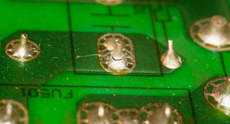
- Non-wetting, or false welding, is also called “weld welding.” Some people also use the term “false soldering,” which can be confusing to foreigners. Non-wetting is usually used to describe the appearance of welding, which looks like tin to the naked eye but did not weld correctly.

- Cold soldering: cold solder, in the definition from [IPC-A-610], should also be called non-wetting. That is because of the lack of proper temperature, resulting in poor welding.
- Incomplete weld: I believe that it should be “cold welding.” The parts of the legs appear to be welded, but in fact, the solder does not completely weld the solder feet to the pads or parts of the pads. It just looks like it`s connected, but it is usually possible to observe whether the angle between the solder and the circuit board or the foot, exceeds 90° to judge whether the welding is effective.

- Solder bridge: a phenomenon known as a solder short that is often used to describe a short circuit between IC legs.

- Solder insufficiency: an insufficient amount of tin may affect the soldering strength.
- Whisker: tin whiskers are particularly relevant to look out for in lead-free processes, especially pure tin processes because they are easier to produce than in lead-based methods.
- Component shifted: the part was offset.
- Tombstone: Also known as “Tombstone,” this term is apt and easy to understand, it is used to describe the shortcomings of parts that stand upright like a gravestone after reflow soldering or soldering machine.

- Wrong polarity: the anode and the cathode are wrong.
If the BGA solder ball is poorly soldered, although it can be described as non-wetting or solder short, you can further define the defects of BGA soldering with more professional terms like HIP (Head-In-Pillow) and NWO (Non-Wet-Open).

The explanation of Non-wetting & De-wetting
In the definition from [IPC-A-610], there are two primary soldering defects: non-wetting and de-wetting. I didn’t understand the difference between these two terms at first, but after studying the definitions from IPC, it is now clear, and I will share my experience here.

Non-wetting: The inability of molten solder to form a metallic bond with the basis metal.
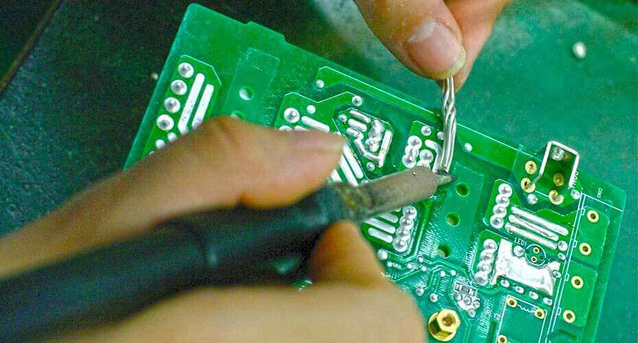
Non-wetting: no wetting occurred, and the parts or pads have insufficient solder. Insufficient temperatures usually cause this issue during soldering. For example, when soldering apart, if one end is connected to a large area of copper foil, the solder pad will not accumulate heat energy to reach the solder temperature because the heat is dissipated too quickly, and so the solder pad gets insufficient soldering. General false welding and cold welding belong to this category. Theoretically, if the solder is well wetting, the angle (θ) between the solder and the circuit board should be less than 90°. If the soldering angle (θ) is greater than 90°, it is usually judged to be Non-wetting.
To solve this type of problem, we can consider preheating the circuit board to get a large area of heat in advance for the copper foil, which will then not absorb the energy of the soldering iron head. Or, design a thermal resistance or thermal relief on the pad to connect the large area copper foil to limit the rapid loss of thermal energy on the pad, it is similar to adding a dam on a river to restrict the water flow.
De-wetting: a condition that results when molten solder coats a surface and then recedes to leave irregularly-shaped mounds of solder that are separated by areas that are covered with a thin film of solder, and with the basis metal or surface finish not exposed.